

High Density Interconnect
High density interconnect, or HDI PCBs are an important component of printed wiring boards (PWB) and electronic circuitry. They allow more components to be fitted in a smaller space, which is why they are so popular in data storage devices and smartphones. The technology behind these devices is also being adopted by the medical industry for use in a variety of applications.
The lifespan of a high density interconnect depends on the environment in which it’s placed, its design, and how well it’s maintained. High-quality components, a skilled manufacturer, and careful installation are critical to the longevity of any device that uses this technology. This is especially true for products that need to perform in a high-speed digital capacity, such as laptops and cell phones.
In addition to reducing the amount of materials required for electronic devices, high-density interconnects can reduce the overall size of a circuit board by allowing more components to be crammed into a small space. This enables manufacturers to create lighter, more compact gadgets that are still capable of meeting the needs and demands of consumers.
The Lifespan of a High Density Interconnect
This advancement in the manufacturing of electronic components has helped to bring new innovations into the world of consumer electronics. It has also allowed for the expansion of the market into emerging countries and markets, and it has enabled advanced technologies such as 5G communication systems, artificial intelligence, and the Internet of Things (IoT) to be integrated into consumer electronics devices.
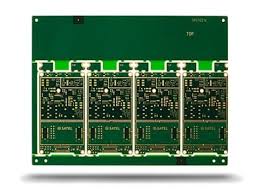
High-density interconnect is a type of printed circuit board that features a number of different components connected to each other through blind and buried vias. These vias are much thinner than traditional through-hole (TH) holes, which allows for more of them to be incorporated into a single board. In addition, they are less likely to degrade over time because they don’t require the same physical support as TH holes.
Another key advantage of high-density interconnect is that it enables more complex circuits to be created in smaller spaces. This can result in devices that are more powerful and efficient than their predecessors. In turn, this has paved the way for innovations like high-resolution video streaming and big-data analytics.
A properly designed HDI PCB can offer up to 2X to 3X more average trace lengths per layer than a standard through-hole PCB, making it a necessary technology when the component pitch requires it or the board size calls for it. This is especially true for high-speed digital and IoT devices, which need the highest possible performance to compete with their competitors in the marketplace.
As a technology that continues to evolve at a rapid pace, high-density interconnect will continue to play an important role in the development of innovative consumer products. However, the intricate nature of high-density PCBs requires that they be designed with specialized expertise and sophisticated tools. In order to meet the unique requirements of this type of design, engineers must take into account a number of factors, including power distribution, signal integrity, and thermal management.