manufacture hdi pcbs
hdi pcbss are used in a wide range of advanced technology systems including smartphones, tablets, games consoles and even medical devices. They offer improved functionality and increased reliability. They also allow the use of smaller components that can be positioned closer together, which results in shorter signal paths and reduced crossing delays. They are designed to withstand high levels of electromagnetic interference (EMI) and have higher impedance tolerance than traditional PCBs.
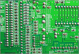
The manufacture of hdi pcbs is a complex process that requires specific fabrication techniques to ensure good manufacturability. This is due to the fact that they are thinner and have more layers than regular PCBs. It is important to understand how these differences affect the manufacturing process so that you can design your PCB correctly. To get the best quality, you should work with a professional PCB manufacturer.
One of the biggest challenges for HDI PCBs is routing vias. It is critical to choose the correct via style for your design and ensure that it can support dense routing without causing signal quality problems. This is because different via styles have different consequences for the signal flow, and a poorly chosen via type can cause significant problems in the finished product.
How do you manufacture hdi pcbs?
In order to produce an HDI PCB, the layers of copper must be separated by an insulating material such as fiberglass or epoxy resin. The layer stackup then undergoes sequential lamination processes where a core of insulated material is combined with copper and the prepreg layers for multi-layer boards before being liquified. This is done with the help of heat and pressure which helps to stick the layers together. Then the layers are drilled by a mechanical drill.
There are two types of HDI PCB structure: build-up/sequential laminations and any-layer structures/every layer interconnect (ELIC). The build-up structure requires that the core is constructed, laminated, drilled, plated, and filled before being laminated with the other layers. The any-layer structure eliminates this step and allows conductors on all layers to be interconnected freely with stacked microvias.
The choice of which structure to use depends on a number of factors, including the ball pitch of the highest pin count device and signal integrity/controlled impedance requirements. In addition, you should consider the layout, layer count, and power and ground requirements of the board. You should also consider the amount of BGA space you need on your circuit board.
Another factor to consider is the fabricator limitations. Fabricators will limit the size of features they can produce, and this will impact your design freedom. This is why it is important to incorporate design for manufacturing (DFM) into your PCB design process from the beginning. This will help you avoid designing a PCB that cannot be manufactured and ensure that the product you are producing will perform as intended.
Manufacture of hdi pcbss involves many complex and time-consuming steps. This includes imaging finer lines and using semiconductor Class 100 clean rooms to reduce defects and rework costs. In addition, it is necessary to take into account the fact that etching and dry film resist are much more demanding than with conventional PCBs. This makes it even more important to choose a professional, experienced PCB manufacturer.