

Verification Revolutionizes PCB Manufacturing Assembly
The production of electronic circuit boards (PCBs) requires utmost precision and accuracy in the entire assembly process. From sourcing components and ensuring that they are compatible with the PCB design to component placement, soldering, and inspection, the assembly of a PCB is highly complex and must be flawless to ensure the quality of the end product.
To streamline the production of a PCB, factories have been adopting automation and robotics for many processes. The implementation of these automated systems has drastically reduced human labor, minimizing errors and streamlining the process. This is done by replacing human operators with automated machines that perform the tasks more accurately than a human. This allows skilled operators to focus on more complicated and demanding tasks, while boosting production speed.
One such automation technology that is revolutionizing the pcb manufacturing assembly is the use of automatic component verification. It is an automated system that detects and confirms the location and orientation of each component on the PCB, allowing for a faster, more accurate production process. This method can be implemented in any stage of the assembly, ensuring that each component is positioned correctly on the PCB before it goes through the reflow soldering process. It can also detect issues like clogged stencil apertures, which can result in solder bridges.
An additional benefit of automated component verification is that it reduces error-prone manual inspection. This is because the accuracy of the machine is far greater than that of a human, which means that there are fewer mistakes made during the inspection process. This automation also eliminates the need to have a human inspect every component, which frees up time for other tasks that can be completed by the factory staff.
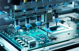
Automated Component Verification Revolutionizes PCB Manufacturing Assembly
This enables factories to increase output while maintaining the same or higher level of quality. It can also help to cut down on rework and waste, which are common in the industry. Moreover, it can make the entire PCB assembly process more efficient by reducing the number of defects that escape inspection.
Automated Optical Inspection (AOI) is a process that utilizes cameras to test the printed circuit board (PCB) for flaws such as missing or incorrectly placed components, open circuits, lifted and misplaced components, soldering difficulties, and stains. AOI is especially useful for multilayer and high-pitch components, which are difficult to inspect with human eyes.
The testing process for a completed PCBA varies depending on the type of product and its reliability requirements. The test process may include a range of different tests, including flying probe and in-circuit testing. An experienced EMS company can create a custom test regimen that is suitable for your specific needs.
While the benefits of automated inspections are numerous, it is important to remember that they can only be effective if you have a strong, well-designed PCB to begin with. This is why choosing a qualified assembly team that specializes in creating precise designs for high-quality, durable, and reliable products is essential.