

Micro Vias Affect the Electrical Properties of a PCB
In PCB design, micro vias are crucial for maximizing connections between layers. Their small size allows for a denser arrangement of connections in a smaller space, supporting the current trends towards thinner and lighter devices with enhanced functionality. But how exactly do they affect the electrical properties of a PCB?
Microvias act as pathways to ensure smooth transmission of power and signals between layers. They are typically used in high-density interconnection (HDI) boards. These vias may be stacked or staggered, and can be filled with conductive epoxy and plated over with copper, or left empty (blind).
The most important factor that determines the performance of a micro vias is its material properties. The conductivity, adhesion and thermal expansion of the material must be carefully considered to optimize microvia performance. This is particularly true for high-speed designs, where the transmission of small, high-frequency signal voltages requires minimal loss.
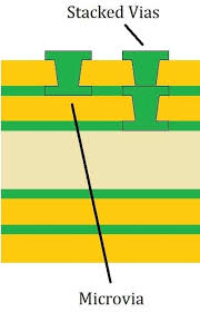
How Do Micro Vias Affect the Electrical Properties of a PCB?
Copper is commonly used to fill a microvia, which offers the advantage of good conductivity. This is critical for ensuring that the currents flowing through it can travel without overtaxing the board and creating heat that could damage components. It’s also helpful in minimizing the effects of parasitic capacitance and inductance, which can distort signal waveforms over long distances.
In addition to its physical attributes, copper is also a good choice for filling a microvia because it has superior thermal conductivity. This is particularly important in a multi-layer circuit board, where the heat generated by high-power components can cause hotspots that can compromise the structural integrity of the assembly.
Another key aspect that influences the performance of a microvia is its geometry. Its diameter must be closely aligned with the diameter of its capture pad, and its aspect ratio should adhere to the IPC’s recommended standard. Deviation from this specification can result in voids that compromise the viability of a microvia and lead to reliability issues.
The quality of a microvia is also determined by its fabrication process. The holes must be thoroughly cleaned after drilling, free of drill smear, fiberglass, inorganic fillers and other debris that can negatively impact the integrity of the via’s plating layer. In addition, the manufacturing process must be able to accommodate fluctuations in the thermal expansion of the substrate and the copper plating.
As a result of the increased density and complexity of modern electronic devices, utilizing microvias is an increasingly popular option for PCB manufacturers. While they can be challenging to fabricate, the benefits of using them, especially in high-performance designs, can outweigh the drawbacks.
Microvias are an ideal solution for reducing the amount of manual routing required on a PCB and enabling it to run faster and more reliably. In addition, they help reduce the risk of electromagnetic interference (EMI), a common problem in high-speed circuits caused by signal reflections in conventional vias and the resulting stubs that can attenuate or cancel the original signal. To minimize EMI, the metals used in microvias should be low-loss materials that provide the lowest possible dielectric constant, or Dk.