

Printed Circuit Boards Are Used in Consumer Electronics
Printed circuit boards (PCBs) are the backbone of modern electronic devices. They allow signals and power to be routed between all the components of a device without having to run wires through them. These boards are comprised of a rigid substrate that holds the component footprints and etched copper paths of the device’s circuitry, along with metal pads to which components can be soldered.
The traces of a PCB are usually made of copper, although other materials such as aluminium are used in some high-performance designs. The copper traces are made of thin strips or wires, each with a specific function. Some are designed to carry the main signaling lines of a circuit, while others are for power, ground or connection to other layers on the board. Most traces are not visible to the naked eye as they are under the protective layer of solder mask, which gives the board its characteristic green color.
To produce a pcb printed circuit board, the designer must start with a schematic, an outline of the device’s functional logic. This is imported into a PCB design system, which will then give the physical layout of the circuitry. The layout is important, as a well-designed pcb printed circuit board will perform as intended, minimizing electrical noise and heat generation, and ensuring that all the traces are adequately separated. The designer will also need to consider the physical limitations of the circuit board, including connectors and mounting holes.
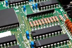
How Printed Circuit Boards Are Used in Consumer Electronics
The layout is drawn on a layer of the substrate, called the base. The base can be one or more insulating layers, such as epoxy resins, fiberglass or phenolics. The most common substrate is FR-4, an epoxy-based laminate. Other types of insulating material include polyimide and polyvinyl chloride (PVC).
A pattern of conductive copper is added to the surface of the board by additive methods such as screen printing or photolithography. To add the copper the bare substrate is coated with a photosensitive film. The exposed film is imaged using light or etching to reveal the areas that will be plated with copper. The unexposed film is then stripped, leaving the copper deposited in the sensitized areas. The remaining bare substrate is then bonded to the copper with epoxy, completing the assembly process.
Some of the drilled holes on a pcb are made conductive, either by electroplating them or by inserting hollow metal eyelets, known as vias. The plated through holes have an annular ring of copper around them. A legend is typically printed on the pcb, often with silkscreen ink. It may contain component designators, switch settings, test points and other indications useful in assembling, testing, servicing and using the device.
A PCB must be able to tolerate the elements it will be subjected to, such as vibration, moisture and physical force. It must also be able to transmit electricity with minimal loss and have a flat dielectric constant.