

Stencil and RF Circuit Board Design
Rf circuit board design involves the use of a series of interconnected components to create a signal that is transmitted and received with high performance. To optimize their performance, RF PCBs require careful layout and component placement to minimize the distance high-frequency signals must travel, which can result in interference and loss. Additionally, RF PCBs must be designed to account for the effect of impedance matching on transmission and reception, which can cause distortion and other problems. One critical element of RF PCB design is the selection of the proper solder paste stencil. A well-designed stencil can significantly improve the efficiency of SMT (Surface Mount Technology) assembly and increase the reliability of the resulting solder joints in subsequent reflow soldering.
The choice of a stencil material depends on the size and type of component being assembled. Smaller components like 0603 capacitors and resistors and 0.02″ pitch SOICs require thinner stencils. Components with a larger package size like 1206 and 0.05″ pitch ICs and capacitors require thicker stencils. Stencils can be made of paper, Mylar, polyimide or stainless steel. They can also be coated with a special nano coating to enhance their printing performance for fine-pitch RF circuits.
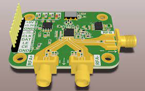
Solder Paste Stencil and RF Circuit Board Design
Before a stencil is used it must be carefully aligned over the pad locations on the rf circuit board design and fixed in place with a vacuum table or other holding mechanism to prevent it from moving during the paste application process. Once the stencil is aligned, a squeegee can be used to apply solder paste evenly across the stencil apertures. It’s important to avoid applying too much solder, which can push paste into vias and corners of pads and create defects during reflow.
Solder paste is a thixotropic material that requires energy in the form of print head motion to change its viscosity and flow evenly into the stencil apertures. The speed setting of the squeegee is critical as it determines how quickly the paste separates from the stencil and onto the pads on the RF circuit board. If the squeegee moves too fast it will deposit excessive amounts of paste and cause defects such as bridging and solder beads.
The design of the RF circuit board must also account for the thickness and arrangement of dielectric and conductive layers to maximize its performance and minimize interference and loss. For example, the thickness of the dielectric layer can be varied to achieve varying degrees of isolation between different conductive paths and to reduce the effect of ground loops. In addition, the conductive path length can be modified to reduce the time it takes for a high-frequency signal to reach its destination and to optimize power transfer. Finally, decoupling capacitors can be placed on the PCB to store charge and filter low-frequency noises. Ideally, they should be connected in parallel to the chip’s Vcc and GND lines.