

Drawbacks of a Via in Pad
A via in pad is a technique used in PCB design to increase the component density of the board. While this is a desirable feature, it comes with its own set of challenges that designers should be aware of when using the technique.
Vias in pads are created by drilling holes in the layers of the circuit board that connect pads on the surface of the circuit board with internal conductors. This allows the use of smaller components on a circuit board since they can be connected directly to internal conductors instead of through copper traces. This can help to reduce the overall size of the circuit board, which is an important consideration for many high-tech electronic devices.
The primary benefit of a via in pad is the ability to increase the component density on a circuit board without increasing the overall thickness. This can be helpful for small devices where space is a concern, such as with BGA technology and fine pitch components.
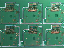
The Benefits and Drawbacks of a Via in Pad
Another benefit of a via in pad is that it can decrease the distance between signal traces on a circuit board. This can help to improve signal integrity, especially for high-speed nets that require more precise routing. This is because the signals must travel less distance and can be influenced less by parasitic inductance that can degrade signal quality over long distances.
Using a via in pad can also simplify routing, especially for large BGA or LGA packages. In these cases, it is possible to avoid solder wicking by filling the via with epoxy before mounting the component to prevent the flow of solder down into the via hole during the reflow process. The epoxy can be filled with either conductive or non-conductive materials. Once the via is filled, it can be capped off with a layer of copper plating to ensure that it provides a good surface for soldering.
One of the drawbacks of a via in pad is that it increases the number of steps involved in the fabrication of the circuit board. This can lead to increased costs and manufacturing defects if not carefully managed.
Additionally, via in pads can lead to thermal stress on components. This is because the pads on the components can melt and detach from the laminate of the circuit board if the via in pad is not properly designed. This can lead to electrical failures in the future.
The most common way to resolve these issues is to use an epoxy filling material that is a low coefficient of thermal expansion (CTE) compared to the laminate on the circuit board. This will prevent the epoxy from moving with or against the circuit board during temperature changes, which can cause stress-induced fractures and electrical failures. This can be done by resist plugging or resin plugging, which can be used together with or before printing the solder mask. Resin plugging is more time consuming than resist plugging and can cause problems with bubbles and out-gassing that may affect the reliability of the circuit board.